
Electroless copper plating process for next-generation semiconductor packages and IC substrates
OPC FLET PROCESS
Semiconductor packaging is advancing rapidly. Key innovations include chiplet technology, 2.5D packaging (which connects multiple chips using silicon bridges inside a substrate), and Fan-Out Panel-Level Packaging (FO-PLP). These advancements require next-generation semiconductor package substrates (IC substrates) to feature finer circuitry and higher connection reliability. However, manufacturers face four major technical challenges.
First, to improve reliability in safety-critical applications like autonomous driving and AI, substrates must ensure crystal continuity at the via-bottom interface and achieve nano-void-free electroless plating films. Second, ultra-fine circuits with Line/Space (L/S) dimensions of 5/5 μm or less require a thinner electroless copper seed layer. This thinness is essential to prevent circuit thinning during flash etching. Third, to minimize transmission loss in high-frequency substrates, manufacturers are using lower-roughness insulating resins. Consequently, the copper must adhere strongly to these smooth surfaces without relying on the physical anchoring effect. Fourth, as insulating resin layers become thinner, haloing (void formation) often occurs between the copper plating and the resin during desmearing and soft etching. We have resolved all four of these challenges.
Our newly developed electroless copper plating process will significantly boost the performance of next-generation semiconductor package substrates and support advanced manufacturing processes.
Product features, specifications
OKUNO's new electroless copper plating process, "OPC FLET PROCESS," addresses these issues by optimizing the catalyst process to deliver a thinner, highly purified electroless copper film. During the recrystallization of the subsequent electrocopper plating film, this advanced process allows the crystals of the plated copper and the inner copper to merge, achieving seamless crystal continuity. It also significantly suppresses the formation of nano-voids at the inner copper interface. Additionally, this thinner electroless copper layer reduces the amount of copper dissolved during flash etching, making fine circuit formation via the semi-additive process (SAP) much easier. Consequently, OPC FLET PROCESS helps resolve "Weak-Micro Via" issues (initial failures and aging failures) caused by fractures between the microvias and the inner copper.
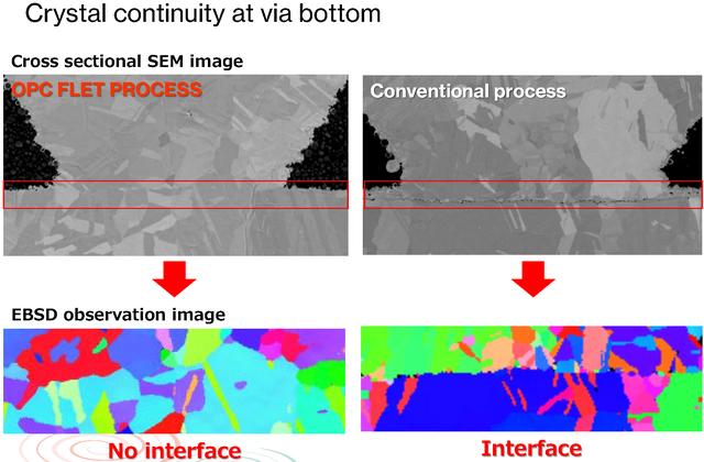
Innovative electroless copper plating process enabling next-generation, high-performance IC substrates
Our new electroless copper plating process, OPC FLET PROCESS, optimizes the catalyzing process resulting in thinner, higher purity electroless copper plating film. This allows for the crystal continuity of the plated copper films and the inner copper layers during the recrystallization of the copper electroplating films.